Small talk about nanotechnology at the Royal Institution

A debate about nanotechnology last Monday at the Royal Institution was run in association with a project called Small Talk, which is planning to run dialogue events about nanotechnology across the UK. This project is a collaboration between the leading organisations in science communication in the UK, The Royal Institution, the British Association, a group of science centres and the Cheltenham Festival of Science. For a science communication organisation they are being a bit reticent, in that they haven’t yet got a web-site up, but I guess we can take this as evidence that nanotechnology has come to the top of the agenda of the science communication professionals.

To be honest, I thought that last Monday’s event actually highlighted some of the problems that this enterprise faces. There are a number of different levels at which one can talk about nanotechnology. You can have a straight discussion about what the technology actually is and what it is likely to become in the near future. At this level, there’s going to be some work to do explaining the basic science, as well as some mentions of the traditional exhibits of contemporary nano-business: tennis rackets, sun-cream, stain resistant trousers etc. You can discuss the debate about what the future holds for the technology, and what the prospects are for the Drexlerian visions. And you can also discuss how one ought to run debates about science and technology and what the right relationship between the public and scientists should be. It’s easy to end up trying to talk about all three, and the result of this is confusion and an unfocused discussion.

While I do applaud James Wilsdon’s notion of an upstream debate, in which people get to discuss technology before it actually arrives, it does take for granted that there are some common assumptions about what the technology actually is. We don’t yet have that common ground when we talk about nanotechnology.
What is this thing called nanotechnology? Part 3. Three phases of nanotechnology

Here I continue my attempt to define what is meant by the term nanotechnology. In Part 1 I tried to define the relevant length-scale, the nanoscale, and in Part 2 I made the distinction between nanoscience and nanotechnology. This leaves us with a definition of nanotechnology that includes any branch of technology that results from our ability to control and manipulate matter on the nanoscale.

This is impossibly broad, and a lot of trouble continues to be caused by people confusing the many very different technologies that are grouped together in this word nanotechnology. I’ve found it useful to break the definition up in the following way (of course the boundaries between the categories are porous and arbitrary):

  • Incremental nanotechnology involves improving the properties of many materials by controlling their nanoscale structure. Plastics, for example, can be reinforced by nanoscale clay particles, making them stronger, stiffer and more chemically resistant. Cosmetics can be formulated in which the oil phase is much more finely dispersed, improving the feel of the product on the skin. Textiles can be coated with nanoscale layers to alter their wetting properties, making them stain-resistant. This kind of nanotechnology is essentially a continuation of existing trends in disciplines like materials science, colloid science and powder technology. Most commercially available products that are said to be based on nanotechnology fall into this category. The science underlying them is sound and the products often are big improvements on what has gone before. However, they do not really represent a decisive break from existing products, many of which already involve nanotechnology as defined this way, even if they aren’t marketed as owing anything to nanotechnology.
  • Evolutionary nanotechnology involves scaling existing technologies down in size to the nanoscale. Here we generally move beyond simple materials that have been redesigned at the nanoscale to functional devices. Such devices could, for example, sense the environment, process information, or convert energy from one form to another. They include nanoscale sensors, which exploit the huge surface area of nanostructured materials like carbon nanotubes to detect environmental contaminants or biochemicals. Other products of evolutionary nanotechnology are semiconductor nanostructures such as quantum dots and quantum wells which are be used to build better solid-state lasers. Another, less well known but potentially important area is in the development of nano-structures that can wrap up molecules and release them under some stimulus; the most obvious use for these is in drug delivery.
  • Radical nanotechnology involves sophisticated nanoscale machines, operating with nanoscale precision. K. Eric Drexler pointed out in Engines of Creation, that we have an existence proof for such a technology in cell biology, which gives us many remarkable examples of such nanoscale machines. Drexler sketched out, in Nanosystems, one particular route to achieve a radical nanotechnology, which involved a mechanical engineering paradigm executed largely in diamond-like carbon. This is often referred to as molecular nanotechnology or MNT. It’s important to realise that MNT isn’t the only conceivable radical nanotechnology. Bionanotechnology refers to an approach in which biological nanomachines are reassembled in artifical contexts, while one can imagine various biomimetic approaches to radical nanotechnology in which design principles from biology are executed in synthetic materials. This sort of approach is the subject of my book Soft Machines.
  • My modest achievement

    At the Royal Institution debate on nanotechnology this evening (about which I’ll write more later) one comment by James Wilsdon, of the think-tank Demos, stuck in my mind:

    “Richard Jones’s work, in Soft Machines, has complexified and problemetised the debate about radical nanotechnology.”

    He assured me afterwards that this was a good thing.

    Soft Machines published in the USA

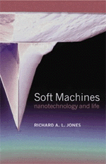
    Soft Machines: nanotechnology and life , by Richard A.L. Jones, is at last published in the USA on October 31 by Oxford University Press. The book is aimed at the general reader, and it explains why things behave differently at the nanoscale to the way they behave at familiar human scales. The book argues that the design principles used by cell biology – the best example we have of a sophisticated working nanotechnology – are particularly well suited to the unfamiliar way physics works at the nanoscale, and that we should try to use the same principles in nanotechnology. Topics discussed include self-assembly in biological and non-biological systems, natural and synthetic molecular motors, molecular electronics and chemical computing.

    Cover of Soft Machines

    Nanotechnology at the Royal Institution

    For anyone in London and at a loose end next Monday, 1 November, there’s an event on at the Royal Institution from 7 pm to 8.30 pm: Nanotechnology: can something so tiny promise something so big?. It’s a debate about nanotechnology and its potential, chaired by the science writer Philip Ball, and featuring myself, Ray Oliver, an industrial nanotechnologist and one of the authors of the recent Royal Society report, and James Wilsdon, from the thinktank Demos, whose recent pamphlet about ways to engage the public about new technologies such as nanotechnology, See-through Science, I wrote about below. It should be an interesting evening.

    A new laboratory for semiconductor nanotechnology at Sheffield

    A suite of refurbished laboratories in my department (Physics and Astronomy, University of Sheffield) was formally opened yesterday by Dame Julia Higgins, chair of EPSRC and Vice President of the Royal Society. The labs were refurbished with money from the Wolfson Foundation and the Royal Society and now house Maurice Skolnick’s work in semiconductor nanotechnology, as well as my own group’s labs. We marked the occasion with a set of scientific seminars.

    It’s always interesting to get an update on what one’s colleagues are up to, and Maurice’s talk had some stunning examples of recent progress in semiconductor nanotechnology. I’ll show just one example.
    Microresonator with quantum dots
    The picture shows (left) a very small diameter photonic micropillar – one can make out a central enclosure, the cavity, sandwiched between two distributed Bragg reflectors (DBRs). These are multilayers of different semiconductors which behave as near-perfect mirrors for light; photons generated inside the cavity are essentially trapped by the mirrors and the edge of the pillar.

    Simply to make these intricately structured micropillars is enough of an achievement (these were made at Sheffield by A Tahraoui and P W Fry). But within the cavity there is a further level of control. The pictures on the right show individual quantum dots, grown by self-assembly. These are incorporated within the cavity of the structure on the left (the transmission electron micrograph, labelled TEM, comes from Hopkinson and Cullis at Sheffield, the scanning tunelling micrograph, labelled STM, from Skolnick’s collaborator P.M. Koenraad at Eindhoven). The resulting structure simultaneously exploits the quantum effects that occur when electrons are confined within the quantum dots, with the optical confinement effects that occur when photons are trapped within the cavity. This allows simultaneous control both of the energies of electronic states in the quantum dot and of the way transitions between electronic states are coupled to the emission of light.

    Quantum dots of this kind are already used to make solid state lasers for use in optical communications. What is really exciting Maurice and his colleagues, though, is the possibility that this kind of structure might be used as the basis for a quantum computer. Quantum computers, if one could get them to work, offer the possibility of massively parallel computing of a power unparalleled with our current CMOS technologies. The problem is that one has to keep quantum states isolated from the environment enough to work their quantum magic, but one still has to retain the ability to interact with the states enough to provide some kind of input and output to the computations. This kind of structure, with its very close control both of the states themselves, and, via the photonic control, of their interactions with the outside world, may just possibly do the trick.

    Then worms ‘ll come and eat thee oop

    I had a late night in the prosperous, liberal, Yorkshire town of Ilkley last night, doing a talk and question and answer session on nanotechnology at the local Cafe Philosophique. An engaged and eclectic audience kept the discussion going well past the scheduled finish time. Two points particularly struck me. One recurring question was whether it was ever realistic to imagine that we can relinquish technological developments with negative consequences – “if it can be done, it will be done” was the comment made more than once. I really don’t like this conclusion, but I’m struggling to find convincing arguments against it. A more positive comment concerned the idea of regulation; we are used to thinking of this idea entirely in terms of narrow prohibitions – don’t release these nanoparticles into the environment, for example. But we need to work out how to make regulation a positive force that steers the technology in a desirable direction, rather than simply trying to sit on it.

    (Non British readers may need to know that the headline is a line from a rather odd and morbid folk-song called “On Ilkley Moor baht hat”, sung mostly by drunken Yorkshiremen.)

    What is this thing called nanotechnology? Part 2. Nanoscience versus Nanotechnology

    In the first part of my attempt to define nanotechnology terms, I discussed definitions of the nanoscale. Now I come to the important and underappreciated distinction between nanoscience and nanotechnology.

    Nanoscience describes the convergence of physics, chemistry, materials science and biology to deal with the manipulation and characterisation of matter on the nanoscale.

    Many subfields of these disciplines have been dealing with nanoscale phenomena for many years. A very non-exhaustive list of relevant sub-fields, with examples of topics in nanoscience, would include:

  • Colloid science. The characterisation and control of forces between sub-micron particles to control the stability of dispersions.
  • Metallurgy. The control of nanoscale structure to optimise mechanical and other properties – e.g. particle and precipitate hardening.
  • Molecular biology and biophysics. Structural characterisation at atomic resolution first of complex biomolecules, now of assemblies of macromolecules which function as nanomachines.
  • Polymer science. Systems such as block copolymers which self-assemble to form complex nanoscale structures, new architectures like hyperbranched polymers and dendrimers.
  • Semiconductor physics. Nanoscale low dimensional structures like multilayers, wires and dots exploiting quantum effects for new electronic and optoelectronic devices like light emitting diodes and lasers.
  • Supramolecular chemistry. The use of non-covalent interactions to create self-assembled nanoscale structures from molecular components.
  • The distinguishing feature of nanoscience is that increasingly we find methods and techniques from more than one of these existing subfields combined in novel ways.

    Nanotechnology is an engineering discipline which combines methods from nanoscience with the disciplines of economics and the market to create usable and economically viable products.

    Nanoscience and nanotechnology need to be distinguished. Without nanoscience, nanotechnology will not be possible. On the other hand, if you invest money in a nanoscience venture under the impression that it is nanotechnology, you are sure to be disappointed.

    In the next installment, I’ll discuss the various kinds of nanotechnology, from incremental technologies such as shampoos and textile treatments to the more radical visions.

    Training the nanotechnologists of the future

    It’s that time of year when academic corridors are brightened by the influx of students, new and returning. I’m particularly pleased to see here at Sheffield the new intake for the Masters course in Nanoscale Science and Technology that we run jointly with the University of Leeds.

    We’ve got 29 students starting this year; it’s the fourth year that the course has been running and over that time we’ve seen a steady growth in demand. I hope that reflects an appreciation of our approach to teaching the subject.

    My view is that to work effectively in nanotechnology you need two things, First comes the in depth knowledge and problem-solving ability you get from studying a traditional discpline, whether that’s a pure science, like physics and chemistry, or an applied science, like materials science, chemical engineering or electrical engineering. But then you need to learn the languages of many other disciplines, because no physicist or chemist, no matter how talented at their own subject, will be able to make much of a contribution in this area unless they are able to collaborate effectively with people with very different sets of skills. That’s why to teach our course we’ve assembled a team from many different departments and backgrounds; physicists, chemists, materials scientists, electrical engineers and molecular biologists are all represented.

    Of course, the nature of nanotechnology is such that there’s no universally accepted curriculum, no huge textbook of the kind that beginning physicists and chemists are used to. The speed of development of the subject is such that we’ve got to make much more use of the primary research literature than one would for, say, a Masters course in physics. And because nanotechnology should be about practise and commercialisation as well as theory we also refer to the patent literature, something that’s, I think, pretty uncommon in academia.

    In terms of choice of subjects, we’re trying to find a balance between the hard nanotechnology of lithography and molecular beam epitaxy and the soft nanotechnology of self-assembly and bionanotechnology. The book of the course, “Nanoscale Science and Technology”, edited by my colleagues Rob Kelsall, Ian Hamley and Mark Geoghegan, will be published in January next year.

    What is this thing called nanotechnology? Part 1. The Nano-scale.

    Nanotechnology, of course, isn’t a single thing at all. That’s why debates about the subject often descend into mutual incomprehension, as different people use the same word to different things, whether it’s business types talking about fabric treatments, scientists talking about new microscopes, or posthumanists and futurists talking about universal assemblers. I’ve attempted to break the term up a little and separate out the different meanings of the word. I’ll soon put these nanotechology definitions on my website, but I’m going to try out the draft definitions here first. First, the all-important issue of scale.

    Nanotechnologies get their name from a unit of length, the nanometer. A nanometer is one billionth of a metre, but let’s try to put this in context. We could call our everyday world the macroscale. This is the world in which we can manipulate things with our bare hands, and in rough terms it covers about a factor of a thousand. The biggest things I can move about are about half a meter big (if they’re not too dense), and my clumsy fingers can’t do very much with things smaller than half a millimeter.

    We’ve long had the tools to extend the range of human abilities to manipulate matter on smaller scales than this. Most important is the light microscope, which has opened up a new realm of matter – the microscale. Like the macroscale, this also embraces roughly another factor of a thousand in length scales. At the upper end, objects half a millimeter or so in size provide the link with the macroscale; still visible to the naked eye, handling them becomes much more convenient with the help of a simple microscope or even a magnifying glass. At the lower end, the wavelength of light itself, around half a micrometer, gives a lower limit on the size of objects which can be discriminated even with the most sophisticated laboratory light microscope.

    Below the microscale is the nanoscale. If we take as the upper limit of the nanoscale the half-micron or so that represents the smallest object that can be resolved in a light microscope, then another factor of one thousand takes us to half a nanometer. This is a very natural lower limit for the nanoscale, because it is a typical size for a small molecule. The nanoscale domain, then, in which nanotechnology operates, is one in which individual molecules are the building blocks of useful structures and devices.

    These definitions are by the nature arbitrary, and it’s not worth spending a lot of time debating precise limits on length scales. Some definitions – the US National Nanotechnology Initiative provides one example – uses a smaller upper limit of 100 nm. There isn’t really any fundamental reason for choosing this number over any other one, except that this definition carries the authority of President Clinton, who of course is famous for the precision of his use of language. Some other definitions attempt to attach some more precise physical significance to this upper length limit on nanotechnology, by appealing to some length at which finite size effects, usually of quantum origin, become important. This is superficially appealing but unattractive on closer examination, because the relevant length-scale on which these finite size effects become important differs substantially according to the phenomenon being looked at. And this line of reasoning leads to an absurd, but commonly held view, that the nanoscale is simply the length-scale on which quantum effects become important. This is a very unhelpful definition when one thinks about it for longer than a second or two; there are plenty of macroscopic phenomena that you can’t understand without invoking quantum mechanics. Magnetism and the electronic behaviour of semiconductors are two everyday examples. And equally, many interesting nanoscale phenomena, notably virtually all of cell biology, don’t really involve quantum mechanical effects in any direct way.

    So I’m going to stick to these twin definitions – it’s the nanoscale if it’s too small to resolve in an ordinary light microscope, and if it’s bigger than your typical small molecule.