Moore’s Law, past and future

Moore’s Law – and the technology it describes, the integrated circuit – has been one of the defining features of the past half century. The idea of Moore’s law has been invoked in three related senses. In its original form, it was rather a precise prediction about the rate of increase of the number of transistors to be fitted on a single integrated circuit. It’s never been a law – it’s been more of an organising principle for an industry and its supply chain – and thus a self-fulfilling prophecy. In this sense, it’s been roughly true for fifty years – but is now bumping up against physical limits.

In the second sense, Moore’s law is used more loosely as a statement about the increase in computing power, and the reduction of its cost, over time. The assertion is that computing power grows exponentially. This also was true, for a while. From the mid 1980’s to the mid 2000’s, computer power grew at a rate of 50% a year compounded, doubling every two years. In this extraordinary period, there was more than a thousandfold cumulative increase over a couple of decades.

The rate of increase in raw computer power has slowed substantially over the last two decades, following the end of Dennard scaling and the limitations of heat dissipation, but this has been counteracted to some extent by software improvements and the development of architectures specialised for particular applications. For example, the Graphics Processing Units – GPUs – that have emerged as being so important for AI are highly optimised for multiplying large matrices.

In the third sense, Moore’s Law is used as a synecdoche for the more general idea of accelerating change, that the pace of change in technology in general is exponential – or even super-exponential – in character. This of course is a commonplace in airport business books. It underpins the idea of a forthcoming singularity, as a received wisdom in Silicon Valley. The idea of the singularity has been given more salience by the recent rapid progress in artificial intelligence, and the widespread view that superhuman artificial general intelligence will soon be upon us.

In this post, I want to go back to the fundamentals – how much the basic components of computing can be shrunk in size, and what the prospects for future miniaturisation are. But this does directly bear on the question of the prospects increase in computer power, which has taken on new importance, as the material basis of the AI boom. AI has brought us to a new situation; in the classical period of fastest growth of computer power (the 80s and 90s) the supply of computing power was growing exponentially, and the opportunity was to find ways of using that power. Now, with AI, it’s the demand for computing power that is growing exponentially, and the issue is whether supply can match that demand.

Moore’s Law. From Max Roser, Hannah Ritchie, and Edouard Mathieu (2023) – “What is Moore’s Law?” Published online at OurWorldinData.org. Retrieved from: ‘https://ourworldindata.org/moores-law‘ [Online Resource]. Licensed under CC-BY.

A classical depiction of Moore’s law is shown in this plot from Our World in Data – with a logarithmic y-axis, a straight line indicates an exponential growth in the number of transistors in successive generations of microprocessor. The seemingly inexorable upward progress of the line conceals a huge amount of innovation; each upward step was facilitated by research and development of new materials and new processes. It also conceals some significant discontinuities.

For example, the earlier relationship between computer power and number of transistors was broken in the mid-2000s. Before then miniaturisation brought a double benefit – it gave you more transistors on each chip, and in addition each transistor worked faster, because it was smaller. The latter relation – Dennard scaling – broke down, because heat dissipation became a limiting factor

Another fundamental change happened in 2012. The fundamental unit of the modern integrated circuit is the metal oxide silicon field effect transistor – the mosFET. This consists channel of doped silicon, with contacts at either end. The channel is coated with a thin, insulating layer of oxide, on top of which is a metal electrode – the gate. It is the gate which controls the flow of electrical current through the channel. When physical limits meant that the planar mosFET couldn’t be shrunk any more, a new design flipped the channel into the vertical plane, so the transistors took the form of fins standing up from the plane of the silicon chip. Each side of the doped silicon fin is coated by insulating oxide and a metal gate, to form the finFET.

The patterns that make the circuits in integrated circuits are made by lithography – light is shone through a patterned mask onto a photoresist, which is subsequently developed to make the pattern physical. The lower limit on the size of the features that can be patterned in this way is ultimately set by the wavelength of light used. Through the 2010’s, lithography was based on using deep ultraviolet light created by excimer lasers – with a 193 nm wavelength. By 2020, this technique had been squeezed as far as it would go, and the 5 nm process node uses extreme UV, with a wavelength of 13.5 nm. The Dutch company ASML has a monopoly on the tools to produce EUV for lithography, each of which costs more than $100 million; the radiation is created in a metal plasma, and has to be focused entirely by mirrors.

I’ve referred to the 2020 iteration of fabrication technology as the “5 nm process”, following a long-standing industry convention of characterising successive technology generations through a single length. In the days of the planar mosFET, a single parameter characterised the size of each transistor – the gate length. There was a stable relationship between the gate length and the length characterising the node number, and there was a roughly biennial decrease in the node number, from the 1982 1.5µm process that drove the explosion of personal computers, to the 2002 90 nm process of the Pentium 4. But with the replacement of the mosFET by the finFET, circuit geometry changed and the relationship between the node size and actual dimensions of the circuit broke down. In fact, the node size now is best thought of as entirely a marketing device, on the principle that the smaller the number the better.

A better way to describe progress in the scaling down of the size uses an estimate of the minimum possible area for a transistor as the product of the metal pitch, the minimum distance between horizontal interconnects, and the contacted gate pitch, the distance from one transistor’s gate to another’s.

Minimum transistor footprint (product of metal pitch and contacted gate pitch) for successive semiconductor process nodes. Data: (1994 – 2014 inclusive) – Stanford Nanoelectronics Lab, post 2017 and projections, successive editions of the IEEE International Roadmap for Devices and Systems

My plot shows the minimum transistor footprint, calculated in this way, for each process node since 1994 (the 350 nm node). The first five nodes – until 2002 – track the exponential increase in density expected from Moore’s law – the fit represents a transistor density that doubles every 2.2 years. The last three generations of planar mosFET technology – until 2009 – show a slight easing of the pace. The switch to the finFET prolonged the trend for another decade or so. But it’s clear now that the “2 nm” node, being introduced by TSMC this year, confirms a marked levelling off of the pace of miniaturisation. For this node, there has been another change of geometry – finFETs have been replaced by vertical rows of nanowires, each completely surrounded by the metal of the gate electrode – GAA, for “gate all around”.

It has to be stressed that miniaturisation of transistors is far from the only way in which computer power can be increased. A good illustration of this comes from progress in making the ultra-powerful chips that have driven the current AI boom, such as Nvidia’s H100. The H100 itself was actually fabricated by TSMC on the “5 nm” node, the first to use AMSL’s EUV light source for lithography. But, as this article explains, only a fraction of the performance improvements of the H100 over previous generations are attributed to Moore’s law. Much of the improvement comes from more efficient ways of representing numbers and carrying out the arithmetic operations that underlie artificial intelligence.

Another factor of growing importance is in the way individual silicon chips are packaged. Many modern integrated circuits, including the H100, are not a single chip. Instead several individual chips, including both logic and memory, are mounted together on a silicon substrate, with fast interconnects to join them all up. The H100 relies on an TSMC advanced packaging technology known as “Chip on Wafer on Substrate” (CoWoS), and is an example of a “System in Package”.

What does the future hold? The latest (2023) iteration of the IEEE’s International Roadmap for Devices and Systems foresees one more iteration of the Gate All Around architecture. The 2031 node is a refinement of that which stacks two mosFETs on top of each other, one with a p-doped channel, one with an n-doped channel (this combination of p- and n- doped FETs is the fundamental unit of logic gates in CMOS technology – “complementary metal oxide silicon”, hence this is referred to as CFET). This essentially doubles the transistor density. After this, no further shrinking in dimensions is envisaged, so further increases in transistor density are to be obtained by stacking multiple tiers of circuits vertically on the wafer.

So what’s the status of Moore’s law now? I return to the 3 senses in which people talk about Moore’s law – as a technical prediction about the growth in the number of transistors on an integrated circuit, as a more general statement about increasing computer power, and as a shorthand for talking about accelerating technical change in general.

In the first, and strictest, sense, we can be definitive – Moore’s law has run its course. The rate of increase in transistor density has significantly slowed since 2020, and exponential growth with an increasing time constant isn’t exponential any more. The technology in its current form has now begun to hit limits, both physical and economic.

For the second, looser, sense, things are more arguable. Available computing power is still increasing, and we see the outcomes of that in advances such as the development of large language models. But this increased power is coming, less from miniaturisation, more from software, specialised architectures optimised for particular tasks, and advanced packaging of chips in “Systems in Package”. It’s this transition that underlies the fact that Nvidia is worth more as a company than TSMC, even though it’s TSMC that actually manufactures (and packages) the chips.

But I wonder whether these approaches will be subject to diminishing returns, in contrast with the classical period of Moore’s law, when constant, large, fractional returns were repeated year after year for decades, producing orders of magnitude cumulative improvements. We are also seeing as a major source of increasing computer power the brute-force approach of just buying more and more chips, in huge, energy consuming data centres. These kind of increases in computer power are fundamentally linear, rather than exponential, in character, and yet they are trying to meet a demand – largely from AI – which is growing exponentially.

It’s very tempting to take Moore’s law as an emblem of the idea that technological change in general is accelerating exponentially, but I think this is unhelpful. Technology isn’t a single thing that improves at a given rate; there are many technologies, and at a given time some will be accelerating, some will be stagnating, some may even be regressing. As we have seen before, the exponential improvement of a single technology never continues forever; physical or economic limits show up, and growth saturates. Continuous progress needs the continuous introduction of new technologies which can take up the baton of growth from those older technologies, whose growth is stalling.

It should be stressed here that when we talk about the end of Moore’s law, the technology that we are talking about isn’t computing in general – it is this particular way of implementing machine logic, CMOS (complementary metal oxide semiconductor). There are many ways in which we can imagine doing computing – the paradox here is that CMOS has been so successful that it has crowded out alternative approaches, some of which might have significant advantages. For example, we know that CMOS logic uses several orders of magnitude more energy per operation than the theoretical minimum (the Landauer limit).

Finally, it does bear repeating what an extraordinary period the heyday of Moore’s law and Dennard scaling was, with computer power doubling every two years, sustained over a couple of decades to produce a cumulative thousand-fold increase. For those who have lived through that period, it will be difficult to resist the belief that this rate of technological progress is part of the natural order of things.
Optical fibres and the paradox of innovation

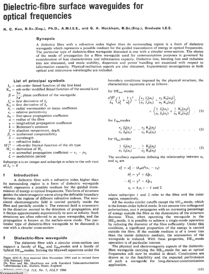
Here is one of the foundational papers for the modern world – in effect, reporting the invention of optical fibres. Without optical fibres, there would be no internet, no on-demand video – and no globalisation, in the form we know it, with the highly dispersed supply chains that cheap and reliable information transmission between nations and continents that optical fibres make possible. This won a Nobel Prize for Charles Kao, a HK Chinese scientist then working in STL in Essex, a now defunct corporate laboratory.

Optical fibres are made of glass – so, ultimately, they come from sand – as Ed Conway’s excellent recent book, “Material World” explains. To make optical fibres a practical proposition needed lots of materials science to make glass pure enough to be transparent over huge distances. Much of this was done by Corning in the USA.

Who benefitted from optical fibres? The value of optical fibres to the world economy isn’t fully captured by their monetary value. Like all manufactured goods, productivity gains have driven their price down to almost negligible levels.

At the moment, the whole world is being wired with optical fibres, connecting people, offices, factories to superfast broadband. Yet, the the world trade in optical fibres is worth just $11 bn, less than 0.05% of total world trade. This is characteristic of that most misunderstood phenomenon in economics, Baumol’s so-called “cost disease”.

New inventions successively transform the economy, while innovation makes their price fall so far that, ultimately, in money terms they are barely detectable in GDP figures. Nonetheless,society benefits from innovations, taken for granted through ubiquity & low cost. (An earlier blog post of mine illustrates how Baumol’s “cost disease” works through a toy model)

To have continued economic growth, we need to have repeated cycles of invention & innovation like this. 30 years ago, corporate labs like STL were the driving force behind innovations like these. What happened to them?

Standard Telecommunication Laboratories in Harlow was the corporate lab of STC, Standard Telephones and Cables, a subsidiary of ITT, with a long history of innovation in electronics, telephony, radio coms & TV broadcasting in the UK. After a brief period of independence from 1982, STC was bought by Nortel, Canadian descendent of the North American Bell System. Nortel needed a massive restructuring after late 90’s internet bubble, & went bankrupt in 2009. The STL labs were demolished & are now a business park

The demise of Standard Communication Laboratories just one example of the slow death of UK corporate laboratories through the 90’s & 00’s, driven by changing norms in corporate governance and growing short-termism. These were well described in the 2012 Kay review of UK Equity Markets and Long-Term Decision Making. This has led, in my opinion, to a huge weakening of the UK’s innovation capacity, whose economic effects are now becoming apparent.

From self-stratifying films to levelling up: A random walk through polymer physics and science policy

After more than two and a half years at the University of Manchester, last week I finally got round to giving an in-person inaugural lecture, which is now available to watch on Youtube. The abstract follows:

How could you make a paint-on solar cell? How could you propel a nanobot? Should the public worry about the world being consumed by “grey goo”, as portrayed by the most futuristic visions of nanotechnology? Is the highly unbalanced regional economy of the UK connected to the very uneven distribution of government R&D funding?

In this lecture I will attempt to draw together some themes both from my career as an experimental polymer physicist, and from my attempts to influence national science and innovation policy. From polymer physics, I’ll discuss the way phase separation in thin polymer films is affected by the presence of surfaces and interfaces, and how in some circumstances this can result in films that “self-stratify” – spontaneously separating into two layers, a favourable morphology for an organic solar cell. I’ll recall the public controversies around nanotechnology in the 2000s. There were some interesting scientific misconceptions underlying these debates, and addressing these suggested some new scientific directions, such as the discovery of new mechanisms for self-propelling nano- and micro- scale particles in fluids. Finally, I will cover some issues around the economics of innovation and the UK’s current problems of stagnant productivity and regional inequality, reflecting on my experience as a scientist attempting to influence national political debates.

It’s the Industrial that enables the Artisanal

It’s come to this, even here. My village chippy has “teamed up” with a “craft brewery” in the next village to sell “artisanal ales” specially brewed to accompany one’s fish and chips. This prompts me to reflect – is this move from the industrial to the artisanal really a reversion to a previous, better world? I don’t think so – instead, craft beer is itself a product of modernity. It depends on capital equipment that is small scale, but dependent on high technology – on stainless steel, electrical heating and refrigeration, computer powered process control. And its ingredients aren’t locally grown and processed – the different flavours introduced by new hop varieties are the outcome of world trade. What’s going on here is not a repudiation of industrialisation, but its miniaturisation, the outcome of new technologies which erode previous economies of scale.

A craft beer from the Eyam Brewery, on sale at the Toll Bar Fish and Chip Shop, Stoney Middleton, Derbyshire.

Beer was one of the first industrial foodstuffs. In Britain, the domestic scale of early beer making began to be replaced by factory scale breweries in the 18th century, as soon as transport improved enough to allow the distribution of their products beyond their immediate locality. Burton-on-Trent was an early centre, whose growth was catalysed by the opening up of the Trent navigation in 1712. This allowed beer to be transported by water via Hull to London and beyond. By the late 18th century some 2000 barrels a year of Burton beer were being shipped to Baltic ports like Danzig and St Petersburg.

Like other process industries, this expansion was driven by fossil fuels. Coal from the nearby Staffordshire and Derbyshire coalfields provided process heat. The technological innovation of coking, which produced a purer carbon fuel which burnt without sulphur containing fumes, was developed as early as 1640 in Derby, so coal could be used to dry malt without introducing off-flavours (this use of coke long predated its much more famous use as a replacement for charcoal in iron production).

By late 19th century, Burton on Trent had become a world centre of beer brewing, producing more than 500 million litres a year, for distribution by the railway network throughout the country and export across the world. This was an industry that was fossil fuel powered and scientifically managed. Coal powered steam engines pumped the large volumes of liquid around, steam was used to provide controllable process heat, and most crucially the invention of refrigeration was the essential enabler of year-round brewing, allowing control of temperature in the fermentation process, by-now scientifically understood by the cadre of formally trained chemists employed by the breweries. In a pint of Marston’s Pedigree or a bottle of Worthington White Shield, what one is tasting is the outcome of the best of 19th century food industrialisation, the mass production of high quality products at affordable prices.

How much of the “craft beer revolution” is a departure from this industrial past? The difference is one of scale – steam engines are replaced by electric pumps, coal fired furnaces by heating elements, and master brewers by thermostatic control systems. Craft beer is not a return to preindustrial, artisanal age – instead it’s based on industrial techniques, miniaturised with new technology, and souped up by the products of world trade. This is a specific example of a point more generally made in Rachel Laudan’s excellent book “Cuisine and Empire” – so-called artisanal food comes after industrial food, and is in fact enabled by it.

What more general lessons can we learn from this example? The energy economy is another place where some people are talking about a transition from a system that is industrial and centralised to one that is small scale and decentralised – one might almost say “artisanal”. Should we be aiming for a new decentralised energy system – a world of windmills and solar cells and electric bikes and community energy trusts?

To some extent, I think this is possible and indeed attractive, leading to a greater sense of control and involvement by citizens in the provision of energy. But we should be under no illusions – this artisanal also has to be enabled by the industrial. Continue reading “It’s the Industrial that enables the Artisanal”

Eroom’s law strikes again

“Eroom’s law” is the name given by pharma industry analyst Jack Scannell to the observation that the productivity of research and development in the pharmaceutical industry has been falling exponentially for decades – discussed in my earlier post Productivity: in R&D, healthcare and the whole economy. The name is an ironic play on Moore’s law, the statement that the number of transistors on an integrated circuit increases exponentially.

It’s Moore’s law that has underlain the orders of magnitude increases in computing power we’ve grown used to. But if computing power has been increasing exponentially, what can we say about the productivity of the research and development effort that’s underpinned those increases? It turns out that in the semiconductor industry, too, research and development productivity has been falling exponentially. Eroom’s law describes the R&D effort needed to deliver Moore’s law – and the unsustainability of this situation must surely play a large part in the slow-down in the growth in computing power that we are seeing now.

Falling R&D productivity has been explicitly studied by the economists Nicholas Bloom, Charles Jones, John Van Reenen and Michael Webb, in a paper called “Are ideas getting harder to find?” (PDF). I discussed an earlier version of this paper here – I made some criticisms of the paper, though I think its broad thrust is right. One of the case studies the economists look at is indeed the electronics industry, and there’s one particular problem with their reasoning that I want to focus on here – though fixing this actually makes their overall argument stronger.

The authors estimate the total world R&D effort underlying Moore’s law, and conclude: “The striking fact, shown in Figure 4, is that research effort has risen by a factor of 18 since 1971. This increase occurs while the growth rate of chip density is more or less stable: the constant exponential growth implied by Moore’s Law has been achieved only by a massive increase in the amount of resources devoted to pushing the frontier forward.”

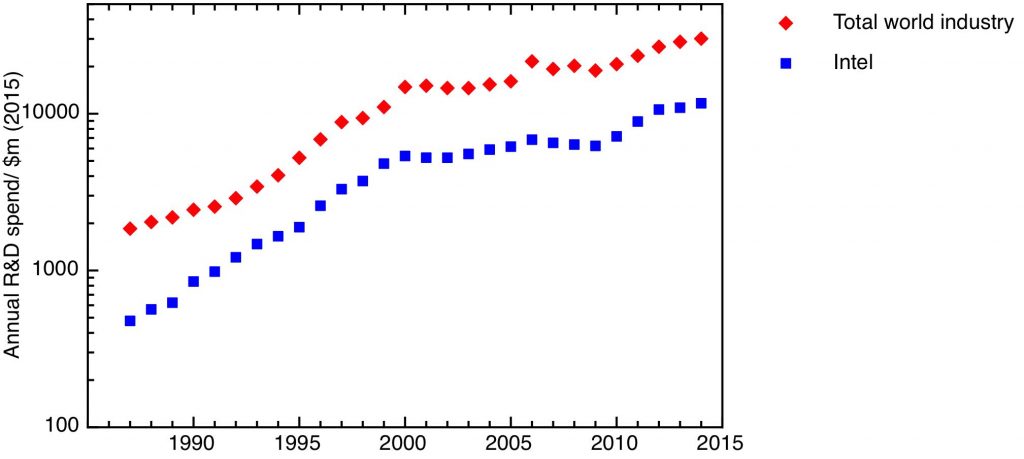
R&D expenditure in the microelectronics industry, showing Intel’s R&D expenditure, and a broader estimate of world microelectronics R&D including semiconductor companies and equipment manufacturers. Data from the “Are Ideas Getting Harder to Find?” dataset on Chad Jones’s website. Inflation corrected using the US GDP deflator.

The growth in R&D effort is illustrated in my first plot, which compares the growth of world R&D expenditure in microelectronics with the growth of computing power. I plot two measures from the Bloom/Jones/van Reenen/Webb data set – the R&D expenditure of Intel, and an estimate of broader world R&D expenditure on integrated circuits, which includes both semiconductor companies and equipment manufacturers (I’ve corrected for inflation using the US GDP deflator). The plot shows an exponential period of increasing R&D expenditure, which levelled off around 2000, to rise again from 2010.

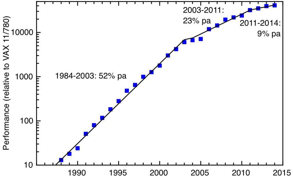
The weakness of their argument, that increasing R&D effort has been needed to maintain the same rate of technological improvement, is that it selects the wrong output measure. No-one is interested in how many transistors there are per chip – what matters to the user, and the wider economy – is that computing power continues to increase exponentially. As I discussed in an earlier post – Technological innovation in the linear age, the fact is that the period of maximum growth in computing power ended in 2004. Moore’s law continued after this time, but the end of Dennard scaling meant that the rate of increase of computing power began to fall. This is illustrated in my second plot. This, after a plot in Hennessy & Patterson’s textbook Computer Architecture: A Quantitative Approach (6th edn) and using their data, shows the relative computing power of microprocessors as a function of their year of introduction. The solid lines illustrate 52% pa growth from 1984 to 2003, 23% pa growth from 2003 – 201, and 9% pa growth from 2011 – 2014.

The growth in processor performance since 1988. Data from figure 1.1 in Computer Architecture: A Quantitative Approach (6th edn) by Hennessy & Patterson.

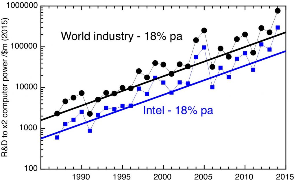
What’s interesting is that the slowdown in the rate of growth in R&D expenditure around 2000 is followed by a slowdown in the rate of growth of computing power. I’ve attempted a direct correlation between R&D expenditure and rate of increase of computing power in my next plot, which plots the R&D expenditure needed to produce a doubling of computer power as a function of time. This is a bit crude, as I’ve used the actual yearly figures without any smoothing, but it does seem to show a relatively constant increase of 18% per year, both for the total industry and for the Intel only figures.

Eroom’s law at work in the semiconductor industry. Real R&D expenditure needed to produce a doubling of processing power as a function of time.

What is the cause of this exponential fall in R&D productivity? A small part reflects Baumol’s cost disease – R&D is essentially a service business done by skilled people, who command wages that reflect the growth of the whole economy rather than their own output (the Bloom et al paper accounts for this to some extent by deflating R&D expenditure by scientific salary levels rather than inflation). But this is a relatively small effect compared to the more general problem of the diminishing returns to continually improving an already very complex and sophisticated technology.

The consequence seems inescapable – at some point the economic returns of improving the technology will not justify the R&D expenditure needed, and companies will stop making the investments. We seem to be close to that point now, with Intel’s annual R&D spend – $12 billion in 2015 – only a little less than the entire R&D expenditure of the UK government, and the projected cost of doubling processor power from here exceeding $100 billion. The first sign has been the increased concentration of the industry. For the 10 nm node, only four companies remained in the game – Intel, Samsung, the Taiwanese foundry company TSMC, and GlobalFoundries, which acquired the microelectronics capabilities of AMD and IBM. As the 7 nm node is being developed, GlobalFoundries has announced that it too is stepping back from the competition to produce next-generation chips, leaving only 3 companies at the technology frontier.

The end of this remarkable half-century of exponential growth in computing power has arrived – and it’s important that economists studying economic growth come to terms with this. However, this doesn’t mean innovation comes to an end too. All periods of exponential growth in particular technologies must eventually saturate, whether that’s as a result of physical or economic limits. In order for economic growth to continue, what’s important is that entirely new technologies must appear to replace them. The urgent question we face is what new technology is now on the horizon, to drive economic growth from here.

The semiconductor industry and economic growth theory

In my last post, I discussed how “econophysics” has been criticised for focusing on exchange, not production – in effect, for not concerning itself with the roots of economic growth in technological innovation. Of course, some of that technological innovation has arisen from physics itself – so here I talk about what economic growth theory might learn from an important episode of technological innovation with its origins in physics – the development of the semiconductor industry.

Economic growth and technological innovation

In my last post, I criticised econophysics for not talking enough about economic growth – but to be fair, it’s not just econophysics that suffers from this problem – mainstream economics doesn’t have a satisfactory theory of economic growth either. And yet economic growth and technological innovation provides an all-pervasive background to our personal economic experience. We expect to be better off than our parents, who were themselves better off than our grandparents. Economics without a theory of growth and innovation is like physics without an arrow of time – a marvellous intellectual construction that misses the most fundamental observation of our lived experience.

Defenders of economics at this point will object that it does have theories of growth, and there are even some excellent textbooks on the subject [1]. Moreover, they might remind us, wasn’t the Nobel Prize for economics awarded this year to Paul Romer, precisely for his contribution to theories of economic growth? This is indeed so. The mainstream approach to economic growth pioneered by Robert Solow regarded technological innovation as something externally imposed, and Romer’s contribution has been to devise a picture of growth in which technological innovation arises naturally from the economic models – the “post-neoclassical endogenous growth theory” that ex-Prime Minister Gordon Brown was so (unfairly) lampooned for invoking.

This body of work has undoubtedly highlighted some very useful concepts, stressing the non-rivalrous nature of ideas and the economic basis for investments in R&D, especially for the day-to-day business of incremental innovation. But it is not a theory in the sense a physicist might understand that – it doesn’t explain past economic growth, so it can’t make predictions about the future.

How the information technology revolution really happened

Perhaps to understand economic growth we need to turn to physics again – this time, to the economic consequences of the innovations that physics provides. Few would disagree that a – perhaps the – major driver of technological innovation, and thus economic growth, over the last fifty years has been the huge progress in information technology, with the exponential growth in the availability of computing power that is summed up by Moore’s law.

The modern era of information technology rests on the solid-state transistor, which was invented by William Shockley at Bell Labs in the late 1940’s (with Brattain and Bardeen – the three received the 1956 Nobel Prize for Physics). In 1956 Shockley left Bell Labs and went to Palo Alto (in what would later be called Silicon Valley) to found a company to commercialise solid-state electronics. However, his key employees in this venture soon left – essentially because he was, by all accounts, a horrible human being – and founded Fairchild Semiconductors in 1957. Key figures amongst those refugees were Gordon Moore – of eponymous law fame – and Robert Noyce. It was Noyce who, in 1960, made the next breakthrough, inventing the silicon integrated circuit, in which a number of transistors and other circuit elements were combined on a single slab of silicon to make a integrated functional device. Jack Kilby, at Texas Instruments, had, more or less at the same time, independently developed an integrated circuit on germanium, for which he was awarded the 2000 Physics Nobel prize (Noyce, having died in 1990, was unable to share this). Integrated circuits didn’t take off immediately, but according to Kilby it was their use in the Apollo mission and the Minuteman ICBM programme that provided a turning point in their acceptance and widespread use[2] – the Minuteman II guidance and control system was the first mass produced computer to rely on integrated circuits.

Moore and Noyce founded the electronics company Intel in 1968, to focus on developing integrated circuits. Moore had already, in 1965, formulated his famous law about the exponential growth with time of the number of transistors per integrated circuit. The next step was to incorporate all the elements of a computer on a single integrated circuit – a single piece of silicon. Intel duly produced the first commercially available microprocessor – the 4004 – in 1971, though this had been (possibly) anticipated by the earlier microprocessor that formed the flight control computer for the F14 Tomcat fighter aircraft. From these origins emerged the microprocessor revolution and personal computers, with its giant wave of derivative innovations, leading up to the current focus on machine learning and AI.

Lessons from Moore’s law for growth economics

What should clear from this very brief account is that classical theories of economic growth cannot account for this wave of innovation. The motivations that drove it were not economic – they arose from a powerful state with enormous resources at its disposal pursuing complex, but entirely non-economic projects – such as the goal of being able to land a nuclear weapon on any point of the earth’s surface with an accuracy of a few hundred meters.

Endogenous growth theories perhaps can give us some insight into the decisions companies made about R&D investment and the wider spillovers that such spending led to. They would need to take account of the complex institutional landscape that gave rise to this innovation. This isn’t simply a distinction between public and private sectors – the original discovery of the transistor was made at Bell Labs – nominally in the private sector, but sustained by monopoly rents arising from government action.

The landscape in which this innovation took place seems much more complex than growth economics, with its array of firms employing undifferentiated labour, capital, all benefiting from some kind of soup of spillovers seems able to handle. Semiconductor fabs are perhaps the most capital intensive plants in the world, with just a handful of bunny-suited individuals tending a clean-room full of machines that individually might be worth tens or even hundreds of millions of dollars. Yet the value of those machines represents, as much as anything physical, the embodied value of the intangible investments in R&D and process know-how.

How are the complex networks of equipment and materials manufacturers coordinated to make sure technological advances in different parts of this system happen at the right time and in the right sequence? These are independent companies operating in a market – but the market alone has not been sufficient to transmit the information needed to keep it coordinated. An enormously important mechanism for this coordination has been the National Technology Roadmap for Semiconductors (later the International Technology Roadmap for Semiconductors), initiated by a US trade body, the Semiconductor Industry Association. This was an important social innovation which allowed companies to compete in meeting collaborative goals; it was supported by the US government by the relaxation of anti-trust law and the foundation of a federally funded organisation to support “pre-competitive” research – SEMATECH.

The involvement of the US government reflected the importance of the idea of competition between nation states in driving technological innovation. Because of the cold war origins of the integrated circuits, the original competition was with the Soviet Union, which created an industry to produce ICs for military use, based around Zelenograd. The degree to which this industry was driven by indigenous innovation as against the acquisition of equipment and know-how from the west isn’t clear to me, but it seems that by the early 1980’s the gap between Soviet and US achievements was widening, contributing to the sense of stagnation of the later Brezhnev years and the drive for economic reform under Gorbachev.

From the 1980’s, the key competitor was Japan, whose electronics industry had been built up in the 1960’s and 70’s driven not by defense, but by consumer products such as transistor radios, calculators and video recorders. In the mid-1970’s the Japanese government’s MITI provided substantial R&D subsidies to support the development of integrated circuits, and by the late 1980’s Japan appeared within sight of achieving dominance, to the dismay of many commentators in the USA.

That didn’t happen, and Intel still remains at the technological frontier. Its main rivals now are Korea’s Samsung and Taiwan’s TSMC. Their success reflects different versions of the East Asian developmental state model; Samsung is Korea’s biggest industrial conglomerate (or chaebol), whose involvement in electronics was heavily sponsored by its government. TSMC was a spin-out from a state-run research institute in Taiwan, ITRI, which grew by licensing US technology and then very effectively driving process improvements.

Could one build an economic theory that encompasses all this complexity? For me, the most coherent account has been Bill Janeway’s description of the way government investment combines with the bubble dynamics that drives venture capitalism, in his book “Doing Capitalism in the Innovation Economy”. Of course, the idea that financial bubbles are important for driving innovation is not new – that’s how the UK got a railway network, after all – but the econophysicist Didier Sornette has extended this to introduce the idea of a “social bubble” driving innovation[3].

This long story suggests that the ambition of economics to “endogenise” innovation is a bad idea, because history tells us that the motivations for some of the most significant innovations weren’t economic. To understand innovation in the past, we don’t just need economics, we need to understand politics, history, sociology … and perhaps even natural science and engineering. The corollary of this is that devising policy solely on the basis of our current theories of economic growth is likely to lead to disappointing outcomes. At a time when the remarkable half-century of exponential growth in computing power seems to be coming to an end, it’s more important than ever to learn the right lessons from history.

[1] I’ve found “Introduction to Modern Economic Growth”, by Daron Acemoglu, particularly useful

[2] Jack Kilby: Nobel Prize lecture, https://www.nobelprize.org/uploads/2018/06/kilby-lecture.pdf

[3] See also that great authority, The Onion “Recession-Plagued Nation Demands New Bubble to Invest In

The Physics of Economics

This is the first of two posts which began life as a single piece with the title “The Physics of Economics (and the Economics of Physics)”. In the first section, here, I discuss some ways physicists have attempted to contribute to economics. In the second half, I turn to the lessons that economics should learn from the history of a technological innovation with its origin in physics – the semiconductor industry.

Physics and economics are two disciplines which have quite a lot in common – they’re both mathematical in character, many of their practitioners are not short of intellectual self-confidence – and they both have imperialist tendencies towards their neighbouring disciplines. So the interaction between the two fields should be, if nothing else, interesting.

The origins of econophysics

The most concerted attempt by physicists to colonise an area of economics is in the area of the behaviour of financial markets – in the field which calls itself “econophysics”. Actually at its origins, the traffic went both ways – the mathematical theory of random walks that Einstein developed to explain the phenomenon of Brownian motion had been anticipated by the French mathematician Bachelier, who derived the theory to explain the movements of stock markets. Much later, the economic theory that markets are efficient brought this line of thinking back into vogue – it turns out that financial markets can be quite often modelled as simple random walks – but not quite always. The random steps that markets take aren’t drawn from a Gaussian distribution – the distribution has “fat tails”, so rare events – like big market crashes – aren’t anywhere like as rare as simple theories assume.

Empirically, it turns out that the distributions of these rare events can sometimes be described by power laws. In physics power laws are associated with what are known as critical phenomena – behaviours such as the transition from a liquid to a gas or from a magnet to a non-magnet. These phenomena are characterised by a certain universality, in the sense that the quantitative laws – typically power laws – that describe the large scale behaviour of these systems doesn’t strongly depend on the details of the individual interactions between the elementary objects (the atoms and molecules, in the case of magnetism and liquids) whose interaction leads collectively to the larger scale phenomenon we’re interested in.

For “econophysicists” – whose background often has been in the study of critical phenomenon – it is natural to try and situate theories of the movements of financial markets in this tradition, finding analogies with other places where power laws can be found, such as the distribution of earthquake sizes and the behaviour of sand-piles. In terms of physicists’ actual impact on participants in financial markets, though, there’s a paradox. Many physicists have found (often very lucrative) employment as quantitative traders, but the theories that academic physicists have developed to describe these markets haven’t made much impact on the practitioners of financial economics, who have their own models to describe market movements.

Other ideas from physics have made their way into discussions about economics. Much of classical economics depends on ideas like the “representative household” or the “representative firm”. Physicists with a background in statistical mechanics recognise this sort of approach as akin to a “mean field theory”. The idea that a complex system is well represented by its average member is one that can be quite fruitful, but in some important circumstances fails – and fails badly – because the fluctuations around the average become as important as the average itself. This motivates the idea of agent based models, to which physicists bring the hope that even simple “toy” models can bring insight. The Schelling model is one such very simple model that came from economics, but which has a formal similarity with some important models in physics. The study of networks is another place where one learns that the atypical can be disproportionately important.

If markets are about information, then physics should be able to help…

One very attractive emerging application of ideas from physics to economics concerns the place of information. Friedrich Hayek stressed the compelling insight that one can think of a market as a mechanism for aggregating information – but a physicist should understand that information is something that can be quantified, and (via Shannon’s theory) that there are hard limits on how much information can transmitted in a physical system . Jason Smith’s research programme builds on this insight to analyse markets in terms of an information equilibrium[1].

Some criticisms of econophysics

How significant is econophysics? A critique from some (rather heterodox) economists – Worrying trends in econophysics – is now more than a decade old, but still stings (see also this commentary from the time from Cosma Shalizi – Why Oh Why Can’t We Have Better Econophysics? ). Some of the criticism is methodological – and could be mostly summed up by saying, just because you’ve got a straight bit on a log-log plot doesn’t mean you’ve got a power law. Some criticism is about the norms of scholarship – in brief: read the literature and stop congratulating yourselves for reinventing the wheel.

But the most compelling criticism of all is about the choice of problem that econophysics typically takes. Most attention has been focused on the behaviour of financial markets, not least because these provide a wealth of detailed data to analyse. But there’s more to the economy – much, much more – than the financial markets. More generally, the areas of economics that physicists have tended to apply themselves to have been about exchange, not production – studying how a fixed pool of resources can be allocated, not how the size of the pool can be increased.

[1] For a more detailed motivation of this line of reasoning, see this commentary, also from Cosma Shalizi on Francis Spufford’s great book “Red Plenty” – “In Soviet Union, Optimization Problem Solves You”.

Between promise, fear and disillusion: two decades of public engagement around nanotechnology

I’m giving a talk with this title at the IEEE Nanotechnology Materials and Devices Conference (NMDC) in Portland, OR on October 15th this year. The abstract is below, and you can read the conference paper here: Between promise, fear and disillusion (PDF).

Nanotechnology emerged as a subject of public interest and concern towards the end of the 1990’s. A couple of decades on, it’s worth looking back at the way the public discussion of the subject has evolved. On the one hand we had the transformational visions associated with the transhumanist movement, together with some extravagant promises of new industries and medical breakthroughs. The flipside of these were worries about profound societal changes for the worse, and, less dramatically, but the potential for environmental and health impacts from the release of nanoparticles.

Since then we’ve seen some real achievements in the field, both scientific and technological, but also a growing sense of disillusion with technological progress, associated with slowing economic growth in the developed world. What should we learn from this experience? What’s the right balance between emphasising the potential of emerging technologies and cautioning against over-optimistic claims?

Read the full conference paper here: Between promise, fear and disillusion (PDF).

Bad Innovation: learning from the Theranos debacle

Earlier this month, Elizabeth Holmes, founder of the medical diagnostics company Theranos, was indicted on fraud and conspiracy charges. Just 4 years ago, Theranos was valued at $9 billion, and Holmes was being celebrated as one of Silicon Valley’s most significant innovators, not only the founder of one of the mythical Unicorns, but through the public value of her technology, a benefactor of humanity. How this astonishing story unfolded is the subject of a tremendous book by the journalist who first exposed the scandal, John Carreyrou. “Bad Blood” is a compelling read – but it’s also a cautionary tale, with some broader lessons about the shortcomings of Silicon Valley’s approach to innovation.

The story of Theranos

The story begins in 2003. Holmes had finished her first year as a chemical engineering student at Stanford. She was particularly influenced by one of her professors, Channing Robertson; she took his seminar on drug delivery devices, and worked in his lab in the summer. Inspired by this, she was determined to apply the principles of micro- and nano- technology to medical diagnostics, and wrote a patent application for a patch which would sample a patient’s blood, analyse it, use the information to determine the appropriate response, and release a controlled amount of the right drug. This closed loop system would combine diagnostics with therapy – hence Theranos, (from “theranostic”).

Holmes dropped out from Stanford in her second year to pursue her idea, encouraged by her professor, Channing Robertson. By the end of 2004, the company she had incorporated, with one of Robertson’s PhD students, Shaunak Roy, had raised $6 million from angels and venture capitalists.

The nascent company soon decided that the original theranostic patch idea was too ambitious, and focused on diagnostics. Holmes focused on the idea of doing blood tests on very small volumes – the droplets of blood you get from a finger prick, rather than the larger volumes you get by drawing blood with a needle and syringe. It’s a great pitch for those scared of needles – but the true promise of the technology was much wider than this. Automatic units could be placed in patients’ homes, cutting out all the delay and inconvenience of having to go to the clinic for the blood draw, and then waiting for the results to come back. The units could be deployed in field situations – with the US Army in Iraq and Afghanistan – or in places suffering from epidemics, like ebola or zika. They could be used in drug trials to continuously monitor patient reactions and pick up side-effects quickly.

The potential seemed huge, and so were the revenue projections. By 2010, Holmes was ready to start rolling out the technology. She negotiated a major partnership with the pharmacy chain Walgreens, and the supermarket Safeway had loaned the company $30 million with a view to opening a chain of “wellness centres”, built around the Theranos technology, in its stores. The US Army – in the powerful figure of General James Mattis – was seriously interested.

In 2013, the Walgreen collaboration was ready to go live; the company had paid Theranos a $100 million “innovation fee” and a $40 million loan on the basis of a 2013 launch. The elite advertising agency Chiat\Day, famous for their work with Apple, were engaged to polish the image of the company – and of Elizabeth Holmes. Investors piled in to a new funding round, at the end of which Theranos was valued at $9 billion – and Holmes was a paper billionaire.

What could go wrong? There turned out to be two flies in the ointment. Firstly, Theranos’s technology couldn’t do even half of what Holmes had been promising, and even on the tests it could do, it was unacceptably inaccurate. Carreyrou’s book is at its most compelling as he gives his own account of how he broke the story, in the face of deception, threats, and some very expensive lawyers. None of this would have come out without some very brave whistleblowers.

At what point did the necessary optimism about a yet-to-be developed technology turn first into self-delusion, and then into fraud? To answer this, we need to look at the technological side of the story.

The technology

As is clear from Carreyrou’s account, Theranos had always taken secrecy about its technology to the point of paranoia – and it was this secrecy that enabled the deception to continue for so long. There was certainly no question that they would be publishing anything about their methods and results in the open literature. But, from the insiders’ accounts in the book, we can trace the evolution of Theranos’s technical approach.

To go back to the beginning, we can get a sense of what was in Holmes’s mind at the outset from her first patent, originally filed in 2003. This patent – “Medical device for analyte monitoring and drug delivery” is hugely broad, at times reading like a digest of everything that anybody at the time was thinking about when it comes to nanotechnology and diagnostics. But one can see the central claim – an array of silicon microneedles would penetrate the skin to extract the blood painlessly, this would be pumped through 100 µm wide microfluidic channels, combined with reagent solutions, and then tested for a variety of analytes through detecting their binding to molecules attached to surfaces. In Holmes’s original patent, the idea was that this information would be processed, and then used to initiate the injection of a drug back into the body. One example quoted was the antibiotic vancomycin, which has rather a narrow window of effectiveness before side effects become severe – the idea would be that the blood was continuously monitored for vancomycin levels, which would then be automatically topped up when necessary.

Holmes and Roy, having decided that the complete closed loop theranostic device was too ambitious, began work to develop a microfluidic device to take a very small sample of blood from a finger prick, route it through a network of tiny pipes, and subject it to a battery of scaled-down biochemical tests. This all seems doable in principle, but fraught with practical difficulties. After three years making some progress, Holmes seems to have decided that this approach wasn’t going to work in time, so in 2007 the company switched direction away from microfluidics, and Shaunak Roy parted from it amicably.

The new approach was based around a commercial robot they’d acquired, designed for the automatic dispensing of adhesives. The idea of basing their diagnostic technology on this “gluebot” is less odd than it might seem. There’s nothing wrong with borrowing bits of technology from other areas, and reliably glueing things together depends on precise, automated fluid handling, just as diagnostic analysis does. But what this did mean was that Theranos no longer aspired to be a microfluidics/nanotech firm, but instead was in the business of automating conventional laboratory testing. This is a fine thing to do, of course, but it’s an area with much more competition from existing firms, like Siemens. No longer could Theranos honestly claim to be developing a wholly new, disruptive technology. What’s not clear is whether its financial backers, or its board, were told enough or had enough technical background to understand this.

The resulting prototype was called Edison 1.0 – and it sort-of worked. It could only do one class of tests – immunoassays, it couldn’t do many of these tests at the same time, and its results were not reproducible or accurate enough for clinical use. To fill in the gaps between what they promised their proprietary technology could do and its actual capabilities, Theranos resorted to modifying a commercial analysis machine – the Siemens Advia 1800 – to be able to analyse smaller samples. This was essential, to fulfil Theranos’s claimed USP, of being able to analyse the drops of blood from pin-pricks rather than the larger volumes taken for standard blood tests from a syringe and needle into a vein.

But these modifications presented their own difficulties. What they amounted to was simply diluting the small blood sample to make it go further – but of course this reduces the concentration of the molecules the analyses are looking for – often below the range of sensitivity of the commercial instruments. And there remained a bigger question, that actually hangs over the viability of the whole enterprise – can one take blood from a pin-prick that isn’t contaminated to an unknown degree by tissue fluid, cell debris and the like? Whatever the cause, it became clear that the test results Theranos were providing – to real patients, by this stage – were erratic and unreliable.

Theranos was working on a next generation analyser – the so-called miniLab – with the goal of miniaturising the existing lab testing methods to make a very versatile analyser. This project never came to fruition. Again, it was unquestionably an avenue worth pursuing. But Theranos wasn’t alone in this venture, and it’s difficult to see what special capabilities they brought that rivals with more experience and a longer track record in this area didn’t have already. Other portable analysers exist already (for example, the Piccolo Xpress), and the miniaturised technologies they would use were already in the market-place (for example, Theranos were studying the excellent miniaturised IR and UV spectrophotometers made by Ocean Optics – used in my own research group). In any case, events had overtaken Theranos before they could make progress with this new device.

Counting the cost and learning the lessons

What was the cost of this debacle? There was an human cost, not fully quantified, in terms of patients being given unreliable test results, which surely led to wrong diagnoses, missed or inappropriate treatments. And there is the opportunity cost – Theranos spent around $900 million, some of this on technology development, but rather too much on fees for lawyers and advertising agencies. But I suspect the biggest cost was the effect Theranos had slowing down and squeezing out innovation in an area that genuinely did have the potential to make a big difference to healthcare.

It’s difficult to read this story without starting to think that something is very wrong with intellectual property law in the United States. The original Theranos patent was astonishingly broad, and given the amount of money they spent on lawyers, there can be no doubt that other potential innovators were dissuaded from entering this field. IP law distinguishes between the conception of a new invention and its necessary “reduction to practise”. Reduction to practise can be by the testing of a prototype, but it can also be by the description of the invention in enough detail that it can be reproduced by another worker “skilled in the art”. Interpretation of “reduction to practise” seems to have become far too loose. Rather than giving the right to an inventor to benefit from a time-limited monopoly on an invention they’ve already got to work, patent law currently seems to allow the well-lawyered to carve out entire areas of potential innovation for their exclusive investigation.

I’m also struck from Carreyrou’s account by the importance of personal contacts in the establishment of Theranos. We might think that Silicon Valley is the epitome of American meritocracy, but key steps in funding were enabled by who was friends with who and by family relationships. It’s obvious that far too much was taken on trust, and far to little actual technical due diligence was carried out.

Carreyrou rightly stresses just how wrong it was to apply the Silicon Valley “fake it till you make it” philosophy to a medical technology company, where what follows from the fakery isn’t just irritation at buggy software, but life-and-death decisions about people’s health. I’d add to this a lesson I’ve written about before – doing innovation in the physical and biological realms is fundamentally more difficult, expensive and time-consuming than innovating in the digital world of pure information, and if you rely on experience in the digital world to form your expectations about innovation in the physical world, you’re likely to come unstuck.

Above all, Theranos was built on gullibility and credulousness – optimism about the inevitability of technological progress, faith in the eminence of the famous former statesmen who formed the Theranos board, and a cult of personality around Elizabeth Holmes – a cult that was carefully, deliberately and expensively fostered by Holmes herself. Magazine covers and TED talks don’t by themselves make a great innovator.

But in one important sense, Holmes was convincing. The availability of cheap, accessible, and reliable diagnostic tests would make a big difference to health outcomes across the world. The biggest tragedy is that her actions have set back that cause by many years.

Technological innovation in the linear age

We’re living in an age where technology is accelerating exponentially, but people’s habits of thought are stuck in an age where progress was only linear. This is the conventional wisdom of the futurists and the Davos-going classes – but it’s wrong. It may have been useful to say this 30 years ago: then we were just starting on an astonishing quarter century of year-on-year, exponential increases in computing power. In fact, the conventional wisdom is doubly wrong – now that that exponential growth in computing power has come to an end, those people who lived through that atypical period are perhaps the least well equipped to deal with what comes next. The exponential age of computing power that the combination of Moore’s law and Dennard scaling gave us, came to an end in the mid-2000’s, but technological progress will continue. But the character of that progress is different – dare I say it, it’s going to be less exponential, more linear. Now, if you need more computer power, you aren’t going to be able to wait for a year or two for Moore’s law to do its work; you’re much more likely to add another core to your CPU, another server to your datacenter. This transition is going to have big implications for business and our economy, which I don’t see being taken very seriously yet.

Just how much faster have computers got? According to the standard textbook on computer architecture, a high-end microprocessor today has nearly 50,000 times the performance of a 1978 mini-computer, at perhaps 0.25% of the cost. But the rate of increase in computing power hasn’t been uniform. A remarkable plot in this book – Computer Architecture: A Quantitative Approach (6th edn) by John Hennessy & David Patterson – makes this clear.

In the early stages of the microprocessor revolution, between 1978 and 1986, computing power was increasing at a very healthy 25% a year – a doubling time of 3 years. It was around 1986 that the rate of change really took off – between 1986 and 2003 computer power increased at an astonishing 52% a year, a doubling time of just a year and a half.

This pace of advance was checked in 2004. The rapid advance had come about from the combination of two mutually reinforcing factors. The well-known Moore’s law dictated the pace at which the transistors in microprocessors were miniaturised. More transistors per chip gives you more computing power. But there was a less well-known factor reinforcing this – Dennard scaling – which says that smaller transistors allow your computer to run faster. It was this second factor, Dennard scaling, which broke down around 2004, as I discussed in a post last year.

With Moore’s law in operation, but Dennard scaling at an end, between 2003 and 2011, computer power counted to grow, but at the slower rate of 23% – back to a 3 year doubling time. But after 2011, according to Hennessy and Patterson, the growth rate slowed further – down to 3.5% a year since 2015. In principle, this corresponds to a doubling time of 20 years – but, as we’ll see, we’re unlikely to see this happen.

This is a generational change in the environment for technological innovation, and as I discussed in my previous post, I’m surprised that it’s economic implications aren’t being discussed more. There have been signs of this stagnation in everyday life – I think people are much more likely to think twice about replacing their four year old lap-top, say, than they were a decade ago, as the benefits of these upgrades get less obvious. But the stagnation has also been disguised by the growth of cloud computing.

The impressive feats of pattern recognition that allow applications like Alexa and Siri to recognise and respond to voice commands provide a good example of the way personal computing devices give the user the impression of great computer power, when in fact the intensive computation that these applications rely on take place, not in the user’s device, but “in the cloud”. What “in the cloud’ means, of course, is that the computation is carried out by the warehouse scale computers that make up the cloud providers’ server farms.

The end of the era of exponential growth in computing power does not, of course, mean the end of innovation in computing. Rather than relying on single, general purpose CPUs to carry out many different tasks, we’ll see many more integrated circuits built with bespoke architectures optimised for specific purposes. The very powerful graphics processing units that were driven by the need to drive higher quality video displays, but which have proved well-suited to the highly parallel computing needs of machine learning are one example. And without automatic speed gains from progress in hardware, there’ll need to be much more attention given to software optimisation.

What will the economic implications be of moving into this new era? The economics of producing microprocessors will change. The cost of CPUs at the moment is dominated by the amortisation of the huge capital cost of the plant needed to make them. Older plants, whose capital costs are already written off, will find their lives being prolonged, so the cost of CPUs a generation or two behind the leading edge will plummet. This collapse in price of CPUs will be a big driver for the “internet of things”. And it will lead to the final end of Moore’s law, as the cost of new generations becomes prohibitive, squeezed between the collapse in price of less advanced processors and the diminishing returns in performance for new generations.

In considering the applications of computers, habits learnt in earlier times will need to be rethought. In the golden age of technological acceleration, between 1986 and 2003, if one had a business plan that looked plausible in principle but that relied on more computer speed than was currently available, one could argue that another few cycles of Moore’s law would soon sort out that difficulty. At the rates of technological progress in computing prevailing then, you’d only need to wait five years or so for the available computing power to increase by a factor of ten.

That’s not going to be the case now. A technology that is limited by the availability of local computing power – as opposed to computer power in the cloud – will only be able to surmount that hurdle by adding more processors, or by waiting for essentially linear growth in computer power. One example of an emerging technology that might fall into this category would be truly autonomous self-driving vehicles, though I don’t know myself whether this is the case.

The more general macro-economic implications are even less certain. One might be tempted to associate the marked slowing in productivity growth that the developed world saw in the mid-2000’s with the breakdown in Dennard scaling and the end of the fastest period of growth in computer power, but I’m not confident that this stacks up, given the widespread rollout of existing technology, coupled with much greater connectivity through broadband and mobile that was happening at that time. That roll-out, of course, has still got further to go.

This paper – by Neil Thompson – does attempt to quantify the productivity hit to ICT using firms caused by the end of Dennard scaling in 2004, finding a permanent hit to total factor productivity of between 0.5 and 0.7 percentage points for those firms that were unable to adapt their software to the new multicore architectures introduced at the time.

What of the future? It seems inconceivable that the end of the biggest driving force in technological progress over the last forty years would not have some significant macroeconomic impact, but I have seen little or no discussion of this from economists (if any readers know different, I would be very interested to hear about it). This seems to be a significant oversight.

Of course, it is the nature of all periods of exponential growth in particular technologies to come to an end, when they run up against physical or economic limits. What guarantees continued economic growth is the appearance of entirely new technologies. Steam power grew in efficiency exponentially through much of the 19th century, and when that growth levelled out (due to the physical limits of Carnot’s law) new technologies – the internal combustion engine and electric motors – came into play to drive growth further. So what new technologies might take over from silicon CMOS based integrated circuits to drive growth from here?

To restrict the discussion to computing, there are at least two ways of trying to look to the future. We can look at those areas where the laws of physics permit further progress, and the economic demand to drive that progress is present. One obvious deficiency of our current computing technology is its energy efficiency – or lack of it. There is a fundamental physical limit on the energy consumption of computing – the Landauer limit – and we’re currently orders of magnitude away from that. So there’s plenty of room at the bottom here, as it were – and as I discussed in my earlier post, if we are to increase the available computing power of the world simply by building more data centres using today’s technology before long this will be using a significant fraction of the world’s energy needs. So much lower power computing is both physically possible and economically (and environmentally) needed.

We can also look at those technologies that currently exist only in the laboratory, but which look like they have a fighting chance of moving into commercial scales sometime soon. Here the obvious candidate is quantum computing; there really does seem to be a groundswell of informed opinion that quantum computing’s time has come. In physics labs around the world there’s a real wave of excitement at that point where condensed matter physics met nanotechnology, in the superconducting properties of nanowires, for example. Experimentalists are chasing the predicted existence of a whole zoo of quasi-particles (that is quantised collective excitations) with interesting properties, with topics such as topological insulators and Majorana fermion states now enormously fashionable. The fact that companies such as Google and Microsoft have been hoovering up the world’s leading research groups in this area give further cause to suspect that something might be going on.

The consensus about quantum computing among experts that I’ve spoken to is that this isn’t going to lead soon to new platforms for general purpose computing (not least because the leading candidate technologies still need liquid helium temperatures), but that it may give users a competitive edge in specialised uses such as large database searches and cryptography. We shall see (though one might want to hesitate before making big long-term bets which rely on current methods of cryptography remaining unbreakable – some cryptocurrencies, for example).

Finally, one should not forget that information and computing isn’t the only place where innovation takes place – a huge amount of economic growth was driven be technological change before computers were invented, and perhaps new non-information based innovation might drive another future wave of economic growth.

For now, what we can say is that the age of exponential growth of computer power is over. It gave us an extraordinary 40 years, but in our world all exponentials come to an end, and we’re now firmly in the final stage of the s-curve. So, until the next thing comes along, welcome to the linear age of innovation.