Less than Moore?

Some years ago, the once-admired BBC science documentary slot Horizon ran a program on nanotechnology. This was preposterous in many ways, but one sequence stands out in my mind. Michio Kaku appeared in front of scenes of rioting and mayhem, opining that “the end of Moore’s Law is perhaps the single greatest economic threat to modern society, and unless we deal with it we could be facing economic ruin.” Moore’s law, of course, is the observation, or rather the self-fulfilling prophecy, that the number of transistors on an integrated circuit doubles about every two years, with corresponding exponential growth in computing power.

As Gordon Moore himself observes in a presentation linked from the Intel site, “No Exponential is Forever … but We can Delay Forever (2 MB PDF). Many people have prematurely written off the semiconductor industry’s ability to maintain, over forty years, a record of delivering a nearly constant, year on year, percentage shrinking in circuits and increase in computing power. Nonetheless, there will be limits to how far the current CMOS-based technology can be pushed. These limits could arise from fundamental constraints of physics or materials science, or from engineering problems like the difficulties of managing the increasingly problematic heat output of densely packed components, or simply from the economic difficulties of finding business models that can make money in the face of the exponentially increasing cost of plant. The question, then, is not if Moore’s law, for conventional CMOS devices, will run out, but when.

What has underpinned Moore’s law is the International Technology Roadmap for Semiconductors, a document which effectively choreographs the research and development required to deliver the continual incremental improvements on our current technology that are needed to keep Moore’s law on track. It’s a document that outlines the requirements for an increasingly demanding series of linked technological breakthroughs as time marches on; somewhere between 2015 and 2020 a crunch comes, with many problems for which solutions look very elusive. Beyond this time, then, there are three possible outcomes. It could be that these problems, intractable though they look now, will indeed be solved, and Moore’s law will continue through further incremental developments. The history of the semiconductor industry tells us that this possibility should not be lightly dismissed; Moore’s law has already been written off a number of times, only for the creativity and ingenuity of engineers and scientists to overcome what seemed like insuperable problems. The second possibility is that a fundamentally new architecture, quite different from CMOS, will be developed, giving Moore’s law a new lease of life, or even permitting a new jump in computer power. This, of course, is the motivation for a number of fields of nanotechnology. Perhaps spintronics, quantum computing, molecular electronics, or new carbon-based electronics using graphene or nanotubes will be developed to the point of commercialisation in time to save Moore’s law. For the first time, the most recent version of the semiconductor roadmap did raise this possibility, so it deserves to be taken seriously. There is much interesting physics coming out of laboratories around the world in this area. But none of these developments are very close to making it out of the lab into a process or a product, so we need to at least consider the possibility that it won’t arrive in time to save Moore’s law. So what happens if, for the sake of argument, Moore’s law peters out in about ten years time, leaving us with computers perhaps one hundred times more powerful than the ones we have now that take more than a few years to become obsolete. Will our economies collapse and our streets fill with rioters?

It seems unlikely. Undoubtedly, innovation is a major driver of economic growth, and the relentless pace of innovation in the semiconductor industry has contibuted greatly to the growth we’ve seen in the last twenty years. But it’s a mistake to suppose that innovation is synonymous with invention; new ways of using existing inventions can be as great a source of innovation as new inventions themselves. We shouldn’t expect that a period of relatively slow innovation in hardware would mean that there would be no developments in software; on the contrary, as raw computing power gets less superabundant we’d expect ingenuity in making the most of available power to be greatly rewarded. The economics of the industry would change dramatically, of course. As the development cycle lengthened the time needed to amortise the huge capital cost of plant would stretch out and the business would become increasingly commoditised. Even as the performance of chips plateaued, their cost would drop, possibly quite precipitously; these would be the circumstances in which ubiquitous computing truly would take off.

For an analogy, one might want to look a century earlier. Vaclav Smil has argued, in his two-volume history of technology of the late nineteenth and twentieth century (Creating the Twentieth Century: Technical Innovations of 1867-1914 and Their Lasting Impact and Transforming the Twentieth Century: Technical Innovations and Their Consequences ), that we should view the period 1867 – 1914 as a great technological saltation. Most of the significant inventions that underlay the technological achievements of the twentieth century – for example, electricity, the internal combustion engine, and powered flight – were made in this short period, with the rest of the twentieth century being dominated by the refinement and expansion of these inventions. Perhaps we will, in the future, look back on the period 1967 – 2014, in a similar way, as a huge spurt of invention in information and communication technology, followed by a long period in which the reach of these inventions continued to spread throughout the economy. Of course, this relatively benign scenario depends on our continued access to those things on which our industrial economy is truly existentially dependent – sources of cheap energy. Without that, we truly will see economic ruin.

Graphene and the foundations of physics

Graphite, familiar from pencil leads, is a form of carbon consisting of stacks of sheets, each of which consists of a hexagonal mesh of atoms. The sheets are held together only weakly; this is why graphite is such a good lubricant, and when you run a pencil across a piece of paper the mark is made from rubbed off sheets. In 2004, Andre Geim, from the University of Manchester, made the astonishing discovery that you could obtain large, near-perfect sheets of graphite only one atom thick, simply by rubbing graphite against a single crystal silicon substrate – these sheets are called graphene. What was even more amazing was the electronic properties of these sheets – they conduct electricity, and the electrons move through the material at great speed and with very few collisions. There’s been a gold-rush of experiments since 2004, uncovering the remarkable physics of this material. All this has been reviewed in a recent article by Geim and Novosolev (Nature Materials, 6 p 183, 2007) – The rise of graphene (It’s worth taking a look at Geim’s group website, which contains many downloadable papers and articles – Geim is a remarkably creative, original and versatile scientist; besides his discoveries in the graphene field, he’s done very significant work in optical metamaterials and gecko-like nanostructured adhesives, besides his notorious frog-levitation exploits). From the technological point of view, the very high electron mobility of graphene and the possibility of shrinking the dimensions of graphene based devices right down to atomic dimensions make it very attractive as a candidate for electronics when the further miniaturisation of silicon based devices stalls.

At the root of much of the strange physics of graphene is the fact that electrons behave in it like highly relativistic, massless particles. This arises from the way the electrons interact with the regular, 2-dimensional lattice of carbon atoms. Normally when an electron (which we need to think of as a wave, according to quantum mechanics) moves through a lattice of ions, the effect of the way the wave is scattered from the ions and the scattered waves interfere with each other is that the electron behaves as it has a different mass to its real, free space value. But in graphene the effective mass is zero (the energy is simply proportional to the wave-vector, like a photon, rather than being proportional to the wave-vector squared, as would be the case for a normal non-relativistic particle with mass).

The weird way in which electrons in graphene mimic ultra-relativistic particles allows one to test predictions of quantum field theory that would be inaccessible to experiments using fundamental particles. Geim writes about this in this week’s Nature, under the provocative title Could string theory be testable? (subscription needed). Graphene is an example where, from the complexity of the interactions between electrons and a 2-d lattice of ions, simple behaviour emerges, that seems to be well described by the theories of fundamental high energy physics. Geim asks “could we design condensed-matter systems to test the supposedly non-testable predictions of string theory too?” The other question to ask, though, is whether what we think of as the fundamental laws of physics, such as quantum field theory, themselves emerge from some complex inner structure that remains inaccessible to us.

Nobels, Nanoscience and Nanotechnology

It’s interesting to see how various newspapers have reported the story of yesterday’s award of the physics Nobel prize to the discoverers of giant magnetoresistance (GMR). Most have picked up on the phrase used in the press release of the Nobel foundation, that this was “one of the first real applications of the promising field of nanotechnology”. Of course, this begs the question of what’s in all those things listed in the various databases of nanotechnology products, such as the famous sunscreens and stain-resistant fabrics.

References to iPods are compulsory, and this is entirely appropriate. It is quite clear that GMR is directly responsible for making possible the miniaturised hard disk drives on which entirely new product categories, such as hard disk MP3 players and digital video recorders, depend. The more informed papers (notably the Financial Times and the New York Times) have noticed that one name was missing from the award – Stuart Parkin – a physicist working for IBM in Almaden, in California, who was arguably the person who took the basic discovery of GMR and did the demanding science and technology needed to make a product out of it.

The Nobel Prize for Chemistry announced today also highlights the relationship between nanoscience and nanotechnology. It went to Gerhard Ertl, of the Fritz-Haber-Institut in Berlin, for his contributions to surface chemistry. In particular, using the powerful tools of nanoscale surface science, he was able to elucidate the fundamental mechanisms operating in catalysis. For example, he worked out the basic steps of the Haber-Bosch process. A large proportion of the world’s population quite literally depends for their lives on the Haber-Bosch process, which artificially fixes nitrogen from the atmosphere to make the fertilizer on which the high crop yields that feed the world depend.

The two prizes illustrate the complexity of the interaction between science and technology. In the case of GMR, the discovery was one that came out of fundamental solid state physics. This illustrates how what might seem to the scientists involved to be very far removed from applications can, if the effect turns out to be useful, be very quickly be exploited in products (though the science and technology needed to make this transition will itself often be highly demanding, and is perhaps not always appreciated enough). The surface science rewarded in the chemistry prize, by contrast, represents a case in which science is used, not to discover new effects or processes, but to understand better a process that is already technologically hugely important. This knowledge, in turn, can then underpin improvements to the process or the development of new, but analogous, processes.

Giant magnetoresistance – from the iPod to the Nobel Prize

This year’s Nobel Prize for Physics, it was announced today, has been awarded to Albert Fert, from Orsay, Paris, and Peter Grünberg, from the Jülich research centre in Germany, for their discovery of giant magnetoresistance, an effect whereby a structure of layers of alternating magnetic and non-magnetic materials, each only a few atoms thick, has an electrical resistance that is very strongly changed by the presence of a magnetic field.

The discovery was made in 1988, and at first seemed an interesting but obscure piece of solid state physics. But very soon it was realised that this effect would make it possible to make very sensitive magnetic read heads for hard disks. On a hard disk drive, information is stored as tiny patterns of magnetisation. The higher the density of information one is trying to store on a hard drive, the weaker the resulting magnetic field, and so the more sensitive the read head needs to be. The new technology was launched onto the market in 1997, and it is this technology that has made possible the ultra-high density disk drives that are used in MP3 players and digital video recorders, as well as in laptops.

The rapidity with which this discovery was commercialised is remarkable. One probably can’t rely on this happening very often, but this is a salutory reminder that sometimes discoveries can move from the laboratory to a truly industry-disrupting product very quickly indeed, if the right application can be found, and if the underlying technology (in this case the nanotechnology required for making highly uniform films only a few atoms thick) is in place.

Three good reasons to do nanotechnology: 2. For healthcare and medical applications

Part 1 of this series of posts dealt with applications of nanotechnology for sustainable energy. Here I go on to describe why so many people are excited about the possibilities for applying nanotechnology in medicine and healthcare.

It should be no surprise that medical applications of nanotechnology are very prominent in many people’s research agenda. Despite near universal agreement about the desirablility of more medical research, though, there are some tensions in the different visions people have of future nanomedicine. To the general public the driving force is often the very personal experience most people have of illness in themselves or people close to them, and there’s a lot of public support for more work aimed at the well known killers of western world, such as cardiovascular disease, cancer, and degenerative diseases like Alzheimer’s and Parkinson’s. Economic factors, though, are important for those responsible for supplying healthcare, whether that’s the government or a private sector insurer. Maybe it’s a slight exaggeration to say that the policy makers’ ideal would be for people to live in perfect health until they were 85 and then tidily drop dead, but it’s certainly true that the prospect of an ageing population demanding more and more expensive nursing care is one that is exercising policy-makers in a number of prosperous countries. In the developing world, there are many essentially political and economic issues which stand in the way of people being able to enjoy the levels of health we take for granted in Europe and the USA, and matters like the universal provision of clean water are very important. Important though the politics of public health is, the diseases that blight developing world, such as AIDS, tuberculosis and malaria, still present major science challenges. Finally, back in the richest countries of the world, there’s a climate of higher expectations of medicine, where people look to medicine to do more than to fix obvious physical ailments, and to move into the realm of human enhancement and prolonging of life beyond what might formerly be regarded as a “natural” lifespan.

So how can nanotechnology help? There are three broad areas.

1. Therapeutic applications of nanotechnology. An important area of focus for medical applications of nanotechnology has been in the area of drug delivery. This begins from the observation that when a patient takes a conventionally delivered drug, an overwhelmingly large proportion of the administered drug molecules don’t end up acting on the biological systems that they are designed to affect. This is a serious problem if the drug has side effects; the larger the dose that has to be administered to be sure that some of the molecule actually gets to the place where it is needed, the worse these side-effects will be. This is particularly obvious, and harrowing, for the intrinsically toxic molecules the drugs used for cancer chemotherapy. Another important driving force for improving delivery mechanisms is the fact that, rather than the simple and relatively robust small molecules that have been the main active ingredients in drugs to date, we are turning increasingly to biological molecules like proteins (such as monoclonal antibodies) and nucleic acids (for example, DNA for gene therapy and small interfering RNAs). These allow very specific interventions into biological processes, but the molecules are delicate, and are easily recognised and destroyed in the body. To deliver a drug, current approaches include attaching it to a large water soluble polymer molecule which is essentially invisible to the body, or wrapping it up in a self-assembled nanoscale bag – a liposome – formed from soap like molecules like phospholipids or block copolymers. Attaching the drug to a dendrimer – a nanoscale treelike structure which may have a cavity in its centre – is conceptually midway between these two approaches. The current examples of drug delivery devices that have made it into clinical use are fairly crude, but future generations of drug delivery vehicles can be expected to include “stealth” coatings to make them less visible to the body, mechanisms for targeting them to their destination tissue or organ and mechanisms for releasing their payload when they get there. They may also incorporate systems for reporting their progress back to the outside world, even if this is only the passive device of containing some agent that shows up strongly in a medical scanner.

Another area of therapeutics in which nanotechnology can make an impact is in tissue engineering and regenerative medicine. Here it’s not so much a question of making artificial substitutes for tissues or organs; ideally it would be in providing the environment in which a patient’s own cells would develop in such a way as to generate new tissue. This is a question of persuading those cells to differentiate to take up the specialised form of a particular organ. Our cells are social organisms, which respond to chemical and physical signals as they develop and differentiate to produce tissues and organs, and the role of nanotechnology here is to provide an environment (or scaffold) which gives the cells the right physical and chemical signals. Once again, self-assembly is one way forward here, providing soft gels which can be tagged with the right chemical signals to persuade the cells to do the right thing.

2. Diagnostics. Many disease states manifest themselves by the presence of specific molecules, so the ability to detect and identify these molecules quickly and reliably, even when they are present at very low concentrations, would be very helpful for the rapid diagnosis of many different conditions. The relevance of nanotechnology is that many of the most sensitive ways of detecting molecules rely on interactions between the molecule and a specially prepared surface; the much greater importance of the surface relative to the bulk for nanostructured materials makes it possible to make sensors of great sensitivity. Sensors for the levels of relatively simple chemicals, such as glucose or thyroxine, could be integrated with devices that release the chemicals needed to rectify any imbalances (these integrated devices go by the dreadful neologism of “theranostics”); recognising pathogens by recognising stretches of DNA would give a powerful way of identifying infectious diseases without the necessity for time-consuming and expensive culturing steps. One obvious and much pursued goal would be to find a way of reading, at a single molecule level, a whole DNA sequence, making it possible cheaply to obtain an individual’s whole genome.

3. Innovation and biomedical research. A contrarian point of view, which I’ve heard frequently and forcibly expressed by a senior figure from the UK’s pharmaceutical industry, is that the emphasis in nanomedicine on drug delivery is misguided, because fundamentally what it represents is an attempt to rescue bad drug candidates. In this view the place to apply nanotechnology is the drug discovery process itself. It’s a cause for concern for the industry that it seems to be getting harder and more expensive to find new drug candidates, and the hopes that were pinned a few years ago on the use of large scale combinatorial methods don’t seem to be working out. In this view, there should be a move away from these brute force approaches to more rational methods, but this time informed by the very detailed insights into cell biology offered by the single molecule methods of bionanotechnology.

New routes to solar energy: the UK announces more research cash

The agency primarily responsible for distributing government research money for nanotechnology in the UK, the Engineering and Physical Sciences Research Council, announced a pair of linked programmes today which substantially increase the funding available for research into new, nano-enabled routes for harnessing solar energy. The first of the Nanotechnology Grand Challenges, which form part of the EPSRC’s new nanotechnology strategy, is looking for large-scale, integrated projects exploiting nanotechnology to enable cheap, efficient and scalable ways to harvest solar energy, with an emphasis on new solar cell technology. The other call, Chemical and Biochemical Solar Energy Conversion, is focussed on biological fuel production, photochemical fuel production and the underpinning fundamental science that enables these processes. Between the two calls, around £8 million (~ US $16 million) is on offer in the first stage, with more promised for continuations of the most successful projects.

I wrote a month ago about the various ways in which nanotechnology might make solar energy, which has the potential to supply all the energy needs of the modern industrial world, more economically and practically viable. The oldest of these technologies – the dye sensitised nano-titania cell invented by EPFL’s Michael Grätzel – is now moving towards full production, with the company G24 Innovations having opened a factory in Wales, in partnership with Konarka. Other technologies such as polymer and hybrid solar cells need more work to become commercial.

Using solar energy to create, not electricity, but fuel, for example for transportation, is a related area of great promise. Some work is already going on developing analogues to photosynthetic systems for using light to split water into hydrogen. A truly grand challenge here would be to devise a system for photochemically reducing carbon dioxide. Think of a system in which one took carbon dioxide (perhaps from the atmosphere) and combined it with water with the aid of a couple of photons of light to make, say, methanol, which could directly be used in your internal combustion engine powered car. It’s possible in principle, one just has to find the right catalyst….

Nanomechanical computers

A report on the BBC News website yesterday – Antique engines inspire nano chip – discussed a new computer design based on the use of nanoscale mechanical elements, which it described as being inspired by the Victorian grandeur of Babbage’s difference engine. The work referred to comes from the laboratory of Robert Blick of the University of Wisconsin, and is published in the New Journal of Physics as A nanomechanical computer—exploring new avenues of computing (free access).

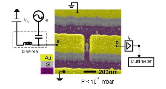
Talk of nanoscale mechanical computers and Babbage’s machine inevitably makes one think of Eric Drexler’s proposals for nanocomputers based on rod logic. However, the operating principles underlying Blick’s proposals are rather different. The basic element is a nanoelectromechanical single electron transistor (a NEMSET, see illustration below). This consists of a silicon nano-post, which oscillates between two electrodes, shuttling electrons between the source and the drain (see also Silicon nanopillars for mechanical single-electron transport (PDF)). The current is a strong function of the applied frequency, because when the post is in mechanical resonance it carries many more electrons across the gap, and the paper demonstrates how coupled NEMSETS can be used to implement logical operations.

Blick stresses that the speed of operation of these mechanical logic gates is not competitive with conventional electronics; the selling points are instead the ability to run at higher temperature (particularly if they were to be fabricated from diamond) and their lower power consumption.

Readers may be interested in Blick’s web-site nanomachines.com, which demonstrates a number of other interesting potential applications for nanostructures fabricated by top-down methods.

The nanoelectromechanical single electron transistor
A nano-electromechanical single electron transistors (NEMSET). From Blick et al., New J. Phys. 9 (2007) 241.

Nanotechnology for solar cells

This month’s issue of Physics World has an useful article giving an overview of the possible applications of nanotechnology to solar cells, under the strapline “Nanotechnology could transform solar cells from niche products to devices that provide a significant fraction of the world’s energy”.

The article discusses both the high road to nano-solar, using the sophistication of semiconductor nanotechnology to make highly efficient (but expensive) solar cells, and the low road, which uses dye-sensitised nanoparticles or semiconducting polymers to make relatively inefficient, but potentially very cheap, materials. One thing the article doesn’t talk about much are the issues of production and scaling, which are currently the main barriers in the way of these materials fully meeting their potential. We will undoubtedly hear much more about this over the coming months and years.

Nanotechnology in the UK news next week

Some high profile events in London next week mean that nanotechnology may move a little way up the UK news agenda. On Monday, there’s an event at the Houses of Parliament: Nano Task Force Conference: Nanotechnology – is Britain leading the way? The Nano Task Force in question is a ginger group set up by Ravi Silva, at the University of Surrey, with political support from Ian Gibson MP. Gibson is a Labour Member of Parliament, one of the rare breed of legislators with a science PhD, and a reputation for being somewhat independent minded.

On Tuesday, public engagement is the theme, with an all-day event “All Talk? Nanotechnologies and public engagement” at the Institute of Physics. This is a joint launch; the thinktank Demos and the Nanotechnology Engagement Group are both launching reports. The Demos report is on a series of public engagement exercises, The Nanodialogues, while Nanotechnology Engagement Group final report is an overview of the lessons learnt from all the engagement activities around nanotechnology conducted so far in the UK. The keynote speaker is Sir David King, the government’s chief scientific advisor.

I’m involved in both, giving a talk on the potential of nanotechnology for sustainable energy on Monday, and Tuesday chairing one session and being a panel member on another. Other participants include Sheila Jasanoff from Harvard, David Edgerton, the author of the recently published book “The Shock of the Old”, Ben Goldacre, the writer of the Guardian’s entertaining ‘Bad science’ column, Andy Stirling, from Sussex, James Wilsdon and Jack Stilgoe from Demos, Doug Parr from Greenpeace, and David Guston, the Director of the Center for Nanotechnology in Society at Arizona State University. It promises to be a fascinating day.